Oto co przeczytacie o Juliuszu Lilienfeldzie w polskiej Wikipedii:
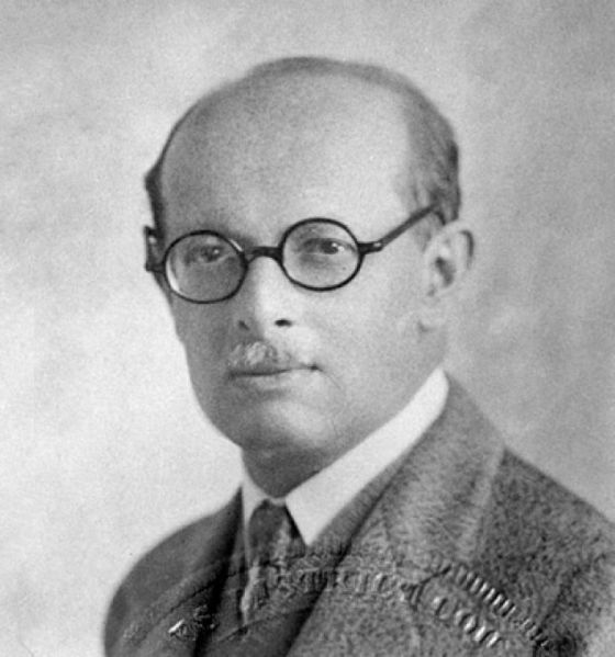
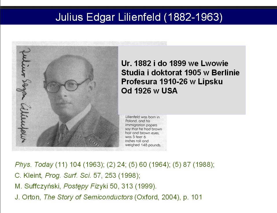
Julius Edgar Lilienfeld (ur. 18 kwietnia 1882 we Lwowie zm. 28 sierpnia 1963) austriacko-węgierski fizyk pochodzenia żydowskiego, twórca tranzystora polowego (podstawowego elementu współczesnych układów cyfrowych).
Syn Siegmunda Lilienfelda, prawnika. W 1899 rozpoczął studia na politechnice w Berlinie, z których po roku zrezygnował. W latach 1900 – 1904 studiował na Uniwersytecie w Berlinie, uzyskując w lutym 1905 roku stopień doktora. W tym samym roku rozpoczął pracę w Instytucie Fizycznym na Uniwersytecie w Lipsku, gdzie habilitował się w 1910.
W 1926 składa wniosek o patent układu będącego protoplastą tranzystora złączowego….”
I tyle. Gdyby on to przeczytał to nieźle skopałby tyłek autorowi tego hasła i temu moderatorowi co je zatwierdzał.
Zacytuję tutaj fragmencik z mojego artykułu poświeconego innemu wielkiemu Polakowi Janowi Czochralskiemu:
“…Jan Czochralski w 1916 r. został autorem genialnego odkrycia – sposobu hodowania dużych monokryształów metali. Współcześnie metodą Czochralskiego hoduje się monokryształy krzemu dla przemysłu półprzewodników. Ale ta metodyka znalazła swoje rewelacyjne zastosowanie dopiero w 50-tych latach, po skonstruowaniu tranzystora przez Waltera Brittaina, Johna Bardeena i Williama Shockleya. Za wynalazek tranzystora cała trójka otrzymała nagrodę Nobla z Fizyki w 1956 roku. Juliusa Lilienfelda pochodzącego spod Lwowa, który uważał się za Polaka pominięto….”
Oto co piszą w English Wiki
Julius Edgar Lilienfeld (April 18, 1882 – August 28, 1963) was an Austro-Hungarian physicist. He was born in Lemberg in Austria-Hungary (now called Lviv in Ukraine), moved to the United States in the early 1920s, and became an American citizen in 1934. Lilienfeld is credited with the first patents on the field effect transistor (1920s) and electrolytic capacitor (1931).
Education
Between 1900 and 1904, Lilienfeld studied at the Friedrich-Wilhelms-Universität (renamed in 1949), in Berlin, where he received his Ph.D. on February 18, 1905. In 1905 he started to work at the physics institute at the University of Leipzig.
Career
Lilienfeld’s early career was at the University of Leipzig, where he conducted important early work on electrical discharges in “vacuum”, between metal electrodes, from about 1910 onwards.[1] His early passion was to clarify how the phenomena changed as vacuum preparation techniques improved. More than any other scientist, he was responsible for the identification of (presently named) field electron emission as a separate physical effect. (He called it “auto-electronic emission”, and was interested in it as a possible electron source for miniaturised X-ray tubes, in medical applications.) Lilienfeld was responsible for the first reliable account in English of the experimental phenomenology of field electron emission, in 1922. The effect itself was explained by Fowler and Nordheim in 1928.
Lilienfeld moved to the United States in the early 1920s, originally in order to defend patents he possessed, and then made a scientific/industrial career there.
Among other things, he invented an “FET-like” transistor and the electrolytic capacitor in the 1920s. He filed several patents describing the construction and operation of transistors as well as many features of modern transistors. (US patent #1,745,175 [2] for an FET-like transistor was granted January 28, 1930.)[3] When Brattain, Bardeen, and Robert Gibney tried to get patents on their earliest devices, most of their claims were rejected due to the Lilienfeld patents.[4]
The optical radiation emitted when electrons are hitting a metal surface is named “Lilienfeld radiation” after he first discovered it close to X-ray tube anodes. Its origin is attributed to the excitation of plasmons in the metal surface.[5][6][7]
The American Physical Society has named one of its major prizes after Lilienfeld.
Personal life
Lilienfeld emigrated to the United States in 1927 and became a US citizen in 1934. He married an American, Beatrice Ginsburg, in New York City on May 2, 1926. They lived in Winchester, Massachusetts, while Lilienfeld was director of the Ergon Research Laboratories in Malden, Massachusetts. In 1935, he and his wife built a house on St. Thomas in the U.S. Virgin Islands in hope of escaping an allergy associated with wheat fields, from which Lilienfeld had suffered for most of his life. Lilienfeld frequently traveled between St. Thomas and various mainland locations and continued to test new ideas and patent the resulting products.
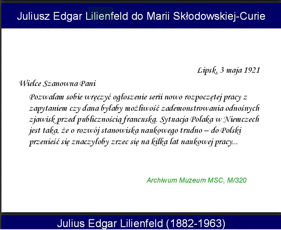
A teraz dowód rzeczowy
List Juliusza Lilienfelda do Marii Skłodowskiej-Curie
Jako naukowca jego biogram funkcjonuje w Jerozolimie, ale nie w Polsce. Jest to jeden z większych skandali na skalę kilku społeczeństw, czyli międzynarodową. postać bezprawnie przywłaszczona przez Żydów i Amerykanów, człowiek skrzywdzony przez Komitet Noblowski szwedzki – Polak , wynalazca tranzystora o którym przede wszystkim zapomniała Polska, a który identyfikował się właśnie z naszym krajem.
Patent:
The Semiconductor Transistor
The modern electronic transistor is a semiconductor device, commonly used to amplify or switch electronic signals. A transistor is made of a solid piece of a semiconductor material, with at least three terminals for connection to an external circuit. A voltage or current applied to one pair of the transistor’s terminals, changes the current flowing through another pair of terminals. Because the controlled (output) power can be much larger than the controlling (input) power, the transistor provides amplification of a signal. The transistor is the fundamental building block of modern electronic devices, and is used in radio, telephone, computer and other electronic systems. Some transistors are packaged individually but most are found in integrated circuits.
As it is often the case with many inventions, the transistor is a result of the work of many inventors, and only the last, or the smartest, takes the all glory. In this case these were the Americans John Bardeen, William Shockley and Walter Brattain, who were presented with the Nobel Prize in Physics in 1956 for their invention of the transistor, which has been called the most important invention of the 20th Century.
Who was the first, however?
The beginning of semiconductor research is marked by Michael Faraday’s 1833 report on negative temperature coefficient of resistance of silver sulfide. This is the first observation of any semiconductor property. In his 1833 paper, “Experimental Researches in Electricity” he disclosed this observation. This observation was in distinction from the usual properties of metals and electrolytes in whose case resistance increase with temperature.
The next significant contributor to semiconductor field is the French experimental physicist Edmond Becquerel. In 1839, he reported the observation of photovoltage in the silver chloride coated platinum electrodes. In his experiment, a AgCl coated platinum electrode was immersed in an aqueous nitric acid electrolyte solution. Illumination of the electrode generated photovoltage that altered the EMF produced by the cell, in fact, it produced a reductive (cathodic) photocurrent at the AgCl coated electrode; this was the first reported photovoltaic device. Photovoltage was generated at the Ag/AgCl metal semiconductor contact.
In 1873, the English electrical engineer Willoughby Smith (1828-1891) arrived at the discovery of photoconductivity of selenium. He was initially working with submarine cables. He set into experiments with selenium for its high resistance, which appeared suitable for his submarine telegraphy. Various experimenters measured the resistance of selenium bars, but the resistance as measured by them under different conditions did not agree at all. Then Smith discovered that the resistance actually depended on the intensity of incident light. When the selenium bars were put inside a box with the sliding cover closed, the resistance was the highest. When glasses of various colors were placed in the way of light, the resistance varied according to the amount of light passing through the glass. But when the cover was removed, the conductivity increased. He also found that the effect was not due to temperature variation.
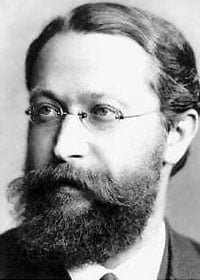 In 1874, the German physicist Ferdinand Braun, a 24-year old graduate of the University of Berlin, studied the characteristics of electrolytes and crystals that conduct electricity at Würzburg University. When he probed a galena crystal (lead sulfide) with the point of a thin metal wire, Braun noted that current flowed freely in one direction only. He had discovered the rectification effect at the point of contact between metals and certain crystal materials.
Braun demonstrated this semiconductor device to an audience at Leipzig on November 14, 1876, but it found no useful application until the advent of radio in the early 1900s when it was used as the signal detector in a “crystal radio” set. The common descriptive name “cat’s-whisker” detector is derived from the fine metallic probe used to make electrical contact with the crystal surface. Braun is better known for his development of the cathode ray tube (CRT) oscilloscope in 1897, known as the “Braun tube” (Braunsche Röhre in German). He shared the 1909 Nobel Prize with Guglielmo Marconi for his contributions to the development of wireless telegraphy, mainly the development of tunable circuits for radio receivers.
 The first man, applied semiconductors for practical purposes, was the Bengali polymath Sir Jagadish Chandra Bose (1858-1937). Jagadish Chandra Bose was a genius physicist, biologist, botanist, archaeologist, and writer of science fiction. To receive the radiation, he used a variety of different metal semiconductor junctions connected to a highly sensitive galvanometer in series. He invented several semiconductor devices, first of which was his Galena detector, which he invented some time during 1894-1898, and demonstrated in Royal Institution Discourse in 1900. In this device, a pair of point contacts (cat whiskers), in this case of galena, was connected in series with a voltage source and a galvanometer. This device could detect any kind of radiation, Hertzian wave, light waves, and other radiation. He called his galena point contact detector an artificial retina (because by suitable arrangement it could be made to detect only light wave), a universal radiometer. Bose later was awarded the first patent for a semiconductor device in the world namely for Galena detector. Among his other pioneering solid-state semiconductor receivers are the spiral spring coherer and iron mercury iron coherer (detector) with a telephone.
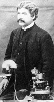
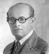
 Between 1902 and 1906, the American Telephone and Telegraph electrical engineer Greenleaf Whittier Pickard (1877-1956) (see the nearby photo) tested thousands of mineral samples to assess their rectification properties. Silicon crystals from Westinghouse yielded some of the best results. On August 20, 1906, he filed a U.S. patent on “Means for receiving intelligent communication by electric waves” for a silicon point-contact detector (diode) and it was awarded that November (see the U.S. patent 836531 of Pickard). With two associates, Pickard founded the Wireless Specialty Apparatus Company to market “cat’s-whisker” crystal radio detectors. It was probably the first company to make and sell silicon semiconductor devices. Another American inventor—Henry Dunwoody received a patent on a system using a point-contact detector made of carborundum (silicon carbide) only several weeks after Pickard.
In 1915 the American physicist Manson Benedicks discovered that a germanium crystal can be used to convert AC (alternating current) current into DC (direct current), i.e. the rectifying properties of germanium crystals. Thus the germanium was added to the list of semiconductors. Till then, it was a short list consisting of silicon, selenium, and tellurium.
In 1927 the Americans L.O. Grondahl and P.H. Geiger invented the copper oxide rectifier. The U.S. Patent 1640335 was issued on August 23rd, 1927, to Grondahl.
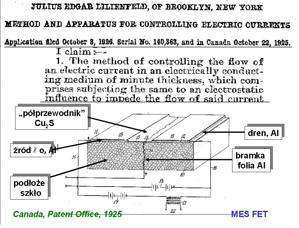
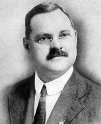
 In 1925 the famous inventor Julius Lilienfeld (see the nearby photo) filed an application for patent in Canada, next year in USA, describing a device, very similar to a MESFET transistor, which he called then Method and Apparatus for Controlling Electric Currents (see the US patent 1745175 of Lilienfeld).
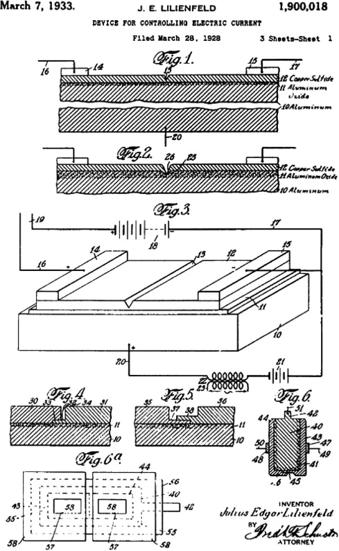
Julius Edgar Lilienfeld (1882–1963) was a remarkable person in the field of physics and electronics. The Austrian Jew Lilienfeld was born in Lemberg in Austria-Hungary (now called Lviv in Ukraine). He was educated (PhD in physics) and lived in Germany till the middle of 1920s, when he decided to emigrate to USA. Besides the abovementioned patent for the first transistor, he was a holder of several other patents in this field—US patent 1900018 “Device for controlling electric current” from 1928 for a thin film MOSFET transistor; US patent 1877140 “Amplifier for electric currents” from 1928, for a solid state device where the current flow is controlled by a porous metal layer, a solid state version of the vacuum tube; US patent 2013564 “Electrolytic condenser” from 1931, for the first electrolytic capacitor. When Brattain, Bardeen and Shockley tried to get a patent on their transistor, most of their claims were rejected namely due to the Lilienfeld patents.
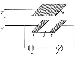 In 1934 another German scientist—Oskar Heil (1908–1994), electrical engineer and inventor, applied for a German patent for an early transistor-like device, describing the possibility of controlling the resistance in a semiconducting material with an electric field, which he called Improvements in or relating to electrical amplifiers and other control arrangements and devices. In 1935 Heil received a British (see the nearby drawing from the Britsh patent), Belgian and French patents for his device.
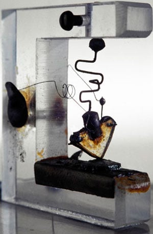 In 1939 William Shockley and Walter Brattain, researchers in Bell Telephone Labs in New Jersey made an unsuccessful attempt to build a semiconductor amplifier by inserting a tiny controlling grid into a layer of copper oxide. The Second World War put an end to their experiments. In 1947 however, the same Brattain, this time together with John Bardeen, invented the point-contact transistor (see the nearby photo of the first transistor, made by germanium). William Shockley (the team’s leader) wasn’t there at the time and did not receive credit for the invention, which pissed him off greatly. It’s just as well. The point-contact transistor was difficult to manufacture and not very reliable. It also wasn’t the transistor that Shockley wanted, so he continued to work on his own idea which led to the junction transistor, which was easier to manufacture and worked better. Bardeen and Brattain filed an application for patent on June 17, 1948 and the patent was issued October 3, 1950 (see the patent).
William Shockley applied for his first patent for the junction transistor at almost the same time—U.S. Patent 2569347 was filed on June 26, 1948 and issued September 25, 1951 (see the first patent of Shockley).
John Bardeen (1908-1991), William Bradford Shockley (1910-1989) and Walter Houser Brattain (1902-1987), (see the lower photo) shared the Nobel Prize in Physics in 1956 “for their researches on semiconductors and their discovery of the transistor effect”.
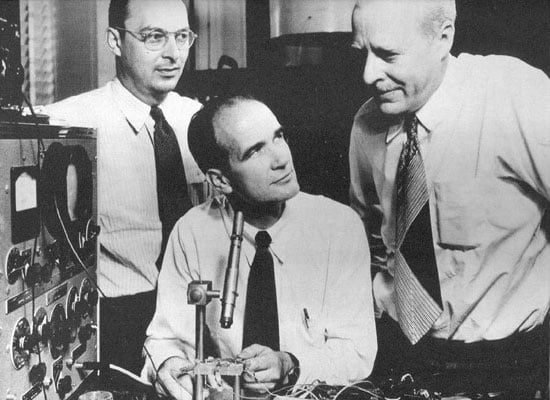
Bardeen (left), Shockley (middle) and Brattain (right)
So how does a transistor work?
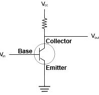 The design of a transistor allows it to function as an amplifier or a switch. This is accomplished by using a small amount of electricity to control a gate on a much larger supply of electricity, much like turning a valve to control a supply of water.
Transistors are composed of three parts, called a base, a collector, and an emitter. The base is the gate controller device for the larger electrical supply. The collector is the larger electrical supply, and the emitter is the outlet for that supply. By sending varying levels of current from the base, the amount of current flowing through the gate from the collector may be regulated. In this way, a very small amount of current may be used to control a large amount of current, as in an amplifier. The same process is used to create the binary code for the digital processors but in this case a voltage threshold of five volts is needed to open the collector gate. In this way, the transistor is being used as a switch with a binary function: five volts—ON, less than five volts—OFF.
Nobel z fizyki
- 1956
-
- William Bradford Shockley
- John Bardeen
- Walter Houser Brattain
- za badania półprzewodników i wynalezienie tranzystora